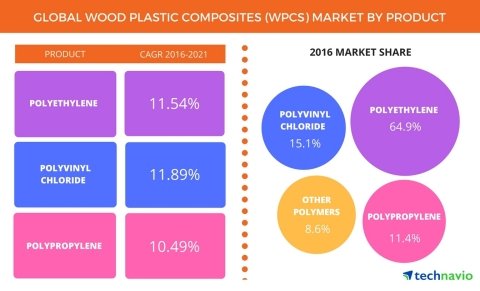
Technavio has published a new report on the global wood plastic composites market from 2017-2021. (Graphic: Business Wire)

Progress in Housing and Building Industries Will Drive the Wooden Plastic Composites Market, Says Technavio

LONDON–(BUSINESS WIRE) – According to the latest market study published by Technavio, the global wood-plastic composite (WPC) market is expected to reach USD 5,991.2 million by 2021 and grow at a CAGR of more than 11%.

This research report, titled Global WPC Market 2017-2021, provides an in-depth analysis of the market in terms of sales and trends in emerging markets. When calculating the market size, the report takes into account sales of WPC products in key applications such as construction, automotive, industrial, and consumer products.

The global WPC market is expected to grow rapidly due to the increased production of composite materials and increasing demand from regions like South America and countries like Russia, China and India. The entry of various suppliers of WPCs is driving consumption in these countries. In August 2015, the GS Group put a pilot WPC production facility into operation in Ulyanovsk, Russia, in which granulated WPC products are to be manufactured that are extruded and injection molded.

Request a sample report: http://www.technavio.com/request-a-sample?report=56938

Technavio’s sample reports are free and include multiple sections of the report including market size and forecast, drivers, challenges, trends, and more.

Technavio’s chemical and materials analysts categorize the global WPC market into four main segments by product type. You are:

  • Polyethylene

  • Polyvinyl chloride

  • Polypropylene

  • Other polymers

The three main product segments for the global WPC market are:

Global market for WPCs made of polyethylene

Polyethylene is one of the widely used thermoplastic polymers. HDPE, low density polyethylene (LDPE), linear LDPE (LLDPE), and ultra high molecular weight polyethylene (UMWPE) are some of the different types of polyethylene available that are suitable for a particular application. In the global WPC market, polyethylene should hold its own well in the forecast period and continue to hold the leading share

Ajay Adikhari, a senior biochemicals and biomaterials analyst for Technavio, said, “The excess availability of recycled HDPE in the US is driving the use of polyethylene as the preferred matrix polymer. On the contrary, PP is the preferred matrix polymer in Europe. Due to the better UV stability of polyethylene, the trend is slowly changing in Europe too. ”

Global Polyvinyl Chloride WPC Market

PVC is a suitable alternative to traditional materials such as glass, copper, iron and wood in various applications because of its operational efficiency and benefits. The polymer has a high hardness and mechanical properties, which improve with increasing molecular weight and lower temperature.

“PVC is made from ethylene, which comes from the oil and gas industry. It can also be made using various hydrocarbons, including derivatives of plants, sugar cane, and coal. PVC matrix WPCs are often used to make windows and are now also used in the terrace segment, ”says Ajay.

Global market for polypropylene WPCs

PP is an unsaturated polyolefin. It is inherently semi-rigid and offers good resistance to chemicals, heat, and fatigue even at high temperatures. PP quality is selected depending on the required specification, processing method and associated costs. Homopolymers, copolymers (5% -15%, ethylene) and random copolymers are the commonly available grades.

Injection molding, blow molding, and general purpose extrusion are some of the widely used processing methods for PP. The development of prototypes on CNC machines and 3D printers with PP matrix is ​​increasing in Europe because these filaments are readily available.

The main vendors highlighted in this report by Technavio’s research analysts are:

  • Advanced Environmental Recycling Technologies (AERT)

  • CPG International

  • Fiberon

  • Trex Company

  • Universal forest products

Browse related reports:

Become a member of Technavio Insights and access all three reports for a fraction of the original cost. As a Technavio Insights member, you have immediate access to new reports as soon as they are published. In addition to all of the 6,000+ existing reports covering segments such as Metals & Minerals, Olefins, and Specialty Chemicals. This subscription will save you thousands while staying connected to Technavio’s ever-changing research library. This enables you to make informed business decisions more efficiently.

About Technavio

Technavio is a leading global technology research and consulting company. The company develops over 2000 research papers each year, covering more than 500 technologies in 80 countries. Technavio has around 300 analysts around the world who specialize in tailor-made consulting and corporate research tasks using the latest cutting-edge technologies.

Technavio analysts use both primary and secondary research techniques to determine the size and vendor landscape in a number of markets. Analysts obtain information using a combination of bottom-up and top-down approaches, as well as internal market modeling tools and proprietary databases. You confirm this data with the data of various market participants and stakeholders along the value chain, including suppliers, service providers, dealers, resellers and end users.

If you are interested in further information, please contact our media team at media@technavio.com.

Source Link

Renegade 3D pen uses plastic bottles and bags as filament

Renegade 3D pen makes use of plastic bottles and luggage as filament

There are several 3D printing pens that use plastic filaments to create 3D structures that you can actually hold in your hands. One of them is the 3Doodler, who we spent time with in January 2015. What they all had in common was that the filaments used tended to be expensive. That has changed with a new 3D pen that is called on Kickstarter and is now called Renegade. This pen can print with these regular filaments, but the really cool part is how you can use plastic from bottles or old bags to create your artistic creations.

The Renegade pen has a screw advance mechanism and heating system. In this way, the pen can transport, destroy and melt the plastic tape made by the ChupaCut plastic bottle shredder. This rotating screw head pushes the plastic forward evenly and extrudes the molten plastic out of the nozzle. The plastic cools down quickly and results in a stable 3D structure.

The manufacturer says the device has “virtually no material limitations”. The pen is designed to use 5-7mm strips cut from PET plastic bottles, plastic bags or plastic files 0.14-0.35mm thick. Standard filaments made of PLA, ABS, nylon, TPE, HIPS, wood and other filaments with a diameter of 1.75 mm can also be used.

The Renegade pen is available in matte black or matte white and has a detachable attachment and a spool for tape. With the ChupaCut 3, 6, 9 or 12 mm plastic bands can be created. The Renegade pen is on Kickstarter and looking for a little over $ 32,000. He has raised over $ 38,000 at the time of writing. The Renegade pen and spool cost about $ 78. If you want the pen along with a ChupaCut bottle shredder, it will cost you around $ 118. A pen, cutter, and fancy stand kit costs $ 131. The dispatch is expected in January.

SOURCE: Kickstarter

Source Link

The filaments from Nefilatek.  Photo via Nefilatek.

Filament startup Nefilatek launches 100% recycled plastic filament

Nefilatek, a Montreal-based startup that specializes in making recycled filaments, has developed 3D printing filaments made from 100% recycled plastic.

The company operates a Kickstarter page where early adopters can choose between two types of filaments: Nefila HIPS (High Impact Polystyrene) Black and Nefila PC (Polycarbonate), which come with reusable spool bobbins and environmentally friendly packaging. With its new filaments, Nefilatek wants to offer a “safe alternative solution for manufacturers, designers and manufacturers” that reduces the amount of plastic that is used and wasted in 3D printing.

The filaments from Nefilatek. Photo via Nefilatek.

Reducing the environmental impact of 3D printing

Nefilatek was founded in 2018 by two engineering students who both admired the capabilities of 3D printing that allowed inventors, product designers, and manufacturers to get their products to market faster, but were disillusioned with the environmental impact of the technology. They founded the company to combat the huge consumption of plastic in the 3D printing industry, a material that is a major environmental pollutant.

Nefilatek claims that the annual plastic consumption from the 3D printing industry is an estimated 30 million pounds, with a projected 250 million pounds by 2020. Currently, according to the company, it is also estimated that the production of 3D printing plastics will result in consumption of 1.4 Million barrels of oil that will generate over 800 million pounds of carbon emissions annually by 2020.

The Nefila HIPS and Nefila PC filaments

Nefilatek’s recycled filaments aim to have “less impact on the planet” for 3D printing. The company’s first filament, Nefila HIPS Black, is made from high-impact polystyrene recycled from Montreal’s electronic waste. The filament’s benefits include impact and heat-resistant 3D prints, while Nefilatek claims it maintains the same properties as standard ABS. The HIPS filament can also be dissolved and smoothed with the sustainable oils D-limonene and turpentine.

The company is currently conducting final testing of its Nefila PC filament extrusion process prior to commercialization. The filament consists of 100% thermoplastic polycarbonate polymers and is geared towards technical applications due to its firm and flexible mechanical properties. It is also resistant to large temperature fluctuations (-50 ° C to + 130 ° C).

Nefilatek is also working on developing a white variant of its Nefila HIPS filament and is also ready to conduct research and development tests on various other materials, including nylon and polypropylene. Since beginning development of its filaments in 2018, Nefilatek launched a Kickstarter in January 2019 to fund further research and development of its filaments with the aim of bringing them to market. The company plans to ship its Kickstarter filament orders in June 2019.

Standard filaments compared to Nefilatek's recycled filament.  Image via Nefilatek.Standard filaments compared to Nefilatek’s recycled filament. Image via Nefilatek.

Filaments made from recycled materials

Several other initiatives have also been launched to help reduce the environmental impact of 3D printing by using recycled materials to make 3D printing filaments. Examples of this are the British brand’s ONE PET filament for 3D printer filaments Filamentous. The company offers a 100% recycled plastic filaments Made from PET plastic bottle waste for end users. ONE PET was produced in collaboration with Tridea, a company that specializes in converting plastic waste into 3D filaments.

In addition, researchers from the US Army Research Laboratory (ARL) have also used Recycled (PET) plastic found in water bottles, yogurt containers, and other recyclable waste materials 3D printing filaments. By using reclaimed materials, service members can quickly use 3D printing to create replacement parts for military vehicles, weapons and equipment.

You can now cast your vote for the third year 3D Printing Industry Awards. Help determine this year’s winners nowand choose the best initiative with 3D printing to create a better world.

Subscribe to the 3D printing industry newsletter for the latest news in additive manufacturing. You can also stay connected by following us Twitter and like us Facebook.

Looking for a career in additive manufacturing? visit 3D print jobs for a selection of roles in the industry.

The picture shown shows filaments from Nefilatek. Photo via Nefilatek.

Source Link

Microwave Electronic Circuits Made via Low-Cost 3D Printer & Plastic Filament - 3DPrint.com

Microwave Digital Circuits Made by way of Low-Value 3D Printer & Plastic Filament – 3DPrint.com

In the electronics industry, 3D printing has been used to make sensors, stretchable electronics, and compliant electronics, and to make waveguide devices and antennas for microwave devices. This is because this technology can be used to design dielectric substrates for certain applications and multilayer devices with multiple dielectric layers that will work with a variety of materials at different densities.

A team of researchers from the Miguel Hernández University of Elche in Spain has published a study entitled “Inexpensive Additive Manufacturing Techniques for Designing Microwave Planar Circuits Using Fused Deposition Modeling”. The paper describes her work with an inexpensive FDM 3D printer and plastic-based filaments to manufacture and implement microwave electronic circuits.

“Since all commercial filaments available for this type of 3D printer are not intended for the implementation of microwave devices, the electrical parameters of each material (dielectric constant and dissipation factor) must be determined. Since FDM does not allow the printing of metallic materials and the conductive filaments currently available do not have high conductivity, it is also necessary for microwave circuits to develop a technique for metallizing 3D printed parts using copper plates attached directly to the substrate, as is the case with conventional high-frequency substrates, ”the researchers wrote. “Due to the manufacturing process of the circuit, which on the one hand includes the manufacture of a substrate on the basis of a pseudo-thermofounded layer of plastic and on the other hand the use of epoxy adhesives to bond the copper plates, it must be checked whether the entire process leads to a reliable structure. “

Prusa i3 BQ Hephestos 3D printer used in this work. (Photo: BQ Hephestos)

For this study, the team selected a low-cost Prusa i3 Hephestos 3D printer that uses extrusion-based FDM (Fused Deposition Modeling) technology. The Cura software was used to adjust the various 3D printing parameters below for all of the materials used.

The researchers analyzed many standard filaments with a diameter of 1.75 mm in order to “obtain different electrical properties for the design of microwave circuits” and selected these for the study:

  • PLA from German RepRap: polymer made from lactic acid molecules
  • ABS from Fillamentum: amorphous, impact-resistant thermoplastic
  • Iglidur I180-PF (Tribo) by Igus: friction-resistant, good response to deterioration in wear
  • ASS from Fillamentum: UV- and water-resistant thermoplastic
  • PLA stainless steel from Protopasta: made of PLA and polished filament made of powdered stainless steel
  • Laybrick filament from CC-PRODUCTS: made of sandstone, offers a surface texture similar to ceramic or stone
  • Taulman nylon 230 filament: synthetic polyamide
  • LayWoo-D3 filament from CC-PRODUCTS: Made from wood fibers and PLA, offers a similar surface texture to wood
  • Smartfil EP filament by Fillamentum: Made from PLA and calcium carbonate, offers a surface texture similar to limestone

As you can see below, the sheets that make up the 3D printed microwave circuit substrates can be classified as either an outer layer or an inner layer. Because the mechanical stiffness of the substrate can be affected by the thickness of the outer layers, the team states that they should be “solid with a fill pattern density percentage of 100%” and made in a linear pattern to reduce surface roughness and avoid porosity . However, it doesn’t matter which fill density or which fill pattern is used for the inner layers.

(a) Structure of the printed layers of the substrates. (b) Linear printing pattern of 3D material with different filling densities, 100%, 50% and 15%.

The 3D printed substrate was metallized by attaching two 35 µm hydraulic pressed copper sheets to each side using a 2216 B / A non-conductive epoxy GRAY adhesive. The researchers built the microwave circuits using a Protomat S42 from the LPKF numerical control milling machine, and once the adhesive has solidified the copper on the substrate, it can be used.

(a) Manufacturing process for printed circuit boards. (b) Printed circuit structure of the various materials.

Manufacturing defects such as bubbles and voids between layers, lack of homogeneity in the layers, or too much adhesive can lead to possible failure of the structural integrity and performance of the 3D printed circuit. To “verify the correct metallization and fabrication of the substrate,” the team used fast and accurate, but inexpensive, ultrasonic non-destructive techniques to perform structural analysis, and turned to the time and frequency domain analysis techniques of circuit C-scans when there were any structural problems or there were defects.

(a) Setup for the measurements of the dielectric permittivity and the loss tangent. (b) Resonator and transmission line on different materials: ABS, PLA and ASA. (c) Electrical properties calculated for different substrates.

In addition, the researchers characterized the electrical properties of each filament in the microwave frequency range and implemented both standard and novel microwave filters in microstrip and stripline technology.

(a) Resonator and transmission line for PLA with densities of 70%, 50% and 15%. (b) Electrical properties for different filling densities of the PLA substrate.

Ultimately, the team designed and manufactured simple planar microwave circuits in a proof-of-concept to demonstrate how feasible it is to use 3D printing for this application.

“The designed devices were manufactured and measured with good results, demonstrating the possibility of using low-cost 3D printers in the design process of microwave planar circuits,” they write.

From left to right, from top to bottom: successive layers within the circuit in steps of approximately 150 µm.

By following this team’s methodology, other researchers could learn to add more complex microwave circuit structures to their work, including designing waveguide filters “using periodic structures where the additive techniques allow the waveguide sections to be designed to obtain higher rejection bandwidth”. and where the correct configuration of the 3D printer enables the design of a “coupling factor of the various filter sections”.

(a) Step impedance filter made with 100% density. (b) Measured and simulated response of the step impedance filter with a substrate with 100% density.

“The ultrasonic structure analysis has shown the reliability of the manufacturing process. In order to check the various possibilities of the additive manufacturing process presented, various simple and complex step impedance filters were finally implemented in microstrip and stripline technology. Both technologies have achieved good results, with better performance when additive options such as different substrate densities are used. Hence, it can be concluded that additive manufacturing techniques offer wide possibilities in the design of planar microwave circuits, ”the researchers concluded.

12